Short ISP: Relay Logic Adder
Purpose
The purpose of this project is to gain a better understanding of how relays work and how early computer logic was able to use relays before the invention of transistors. The end product also aims to be simple and easy to operate for potential students and their parents touring the Design Engineering Studio (DES). Finally, the end product aims to sound pleasing to the ear by performing a series of satisfying mechanical clicks when operated.
The adder is to combine the sum of nine inputs, each of which being a power of two, into a binary output. The maximum sum value is 31. The calculator is capable of producing a possible 32 (25) unique sums (where zero is an acceptable sum). Each switch will add either a 2, 4, 6 or 8 to the total.
| Parts List | |
|---|---|
| 4× Full Adder Custom PCB | 5× DC Power Jack |
| 9× SPDT Toggle Switch | 4× DC Barrel Plug |
| 20W (5V@4A) Power Supply | 5× 10mm Red LED |
| 80× DPDT 5V 2A DC Relay | Grey PLA 3D Printer Filament |
| 6.5" of 1"×1" Square Acrylic tubing | Clear Acrylic Sheet |
| 24× Male/Female Pin Headers | Plywood Board |
Procedure
This project started with choosing relays to be a component in the project through a class Yankee Swap. The planning and idea brainstorming came after choosing relays to be a main component. After researching historic use of relays as logic capable devices, the chosen project would be a modular full adder circuit.
Testing and research on creating logic gates with relays, specifically the NAND logic gate, proceeded the planned idea. NAND gates are important for logic operations as they can create any of the other logic gates when organized in specific ways. This testing and planning is similar to Project 2. Digital (Transistor-Based) Logic Gates, but with relays instead of transistors.
 The next step was creating a half adder with NAND logic using relays. The half adder is a circuit which takes two separate inputs and returns a sum, in binary, of those outputs on two pins, the SUM (Σ) and CARRY OUT pins. For example, if both outputs are high, the sum is a decimal two, represented by a low output on the Σ pin (as there are zero groups of 20) and a high output on the CARRY OUT pin (as there is one group of 21). After testing this circuit and reproducing it in EAGLE, the circuit needed further modifications to transform it into a full adder. Accomplishing this consists of chaining two half adder circuits together and performing a logical OR on the two CARRY OUT pins. The chaining of half adders works by connecting the Σ pin of the first half adder to an input on the second and adding a CARRY IN pin which connects to the second input of the second half adder. Now that a CARRY IN pin is present, the circuit is an operational full adder and it is possible to chain it with other identical full adders to work as a calculator (that only does addition).
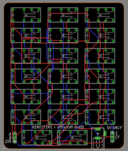
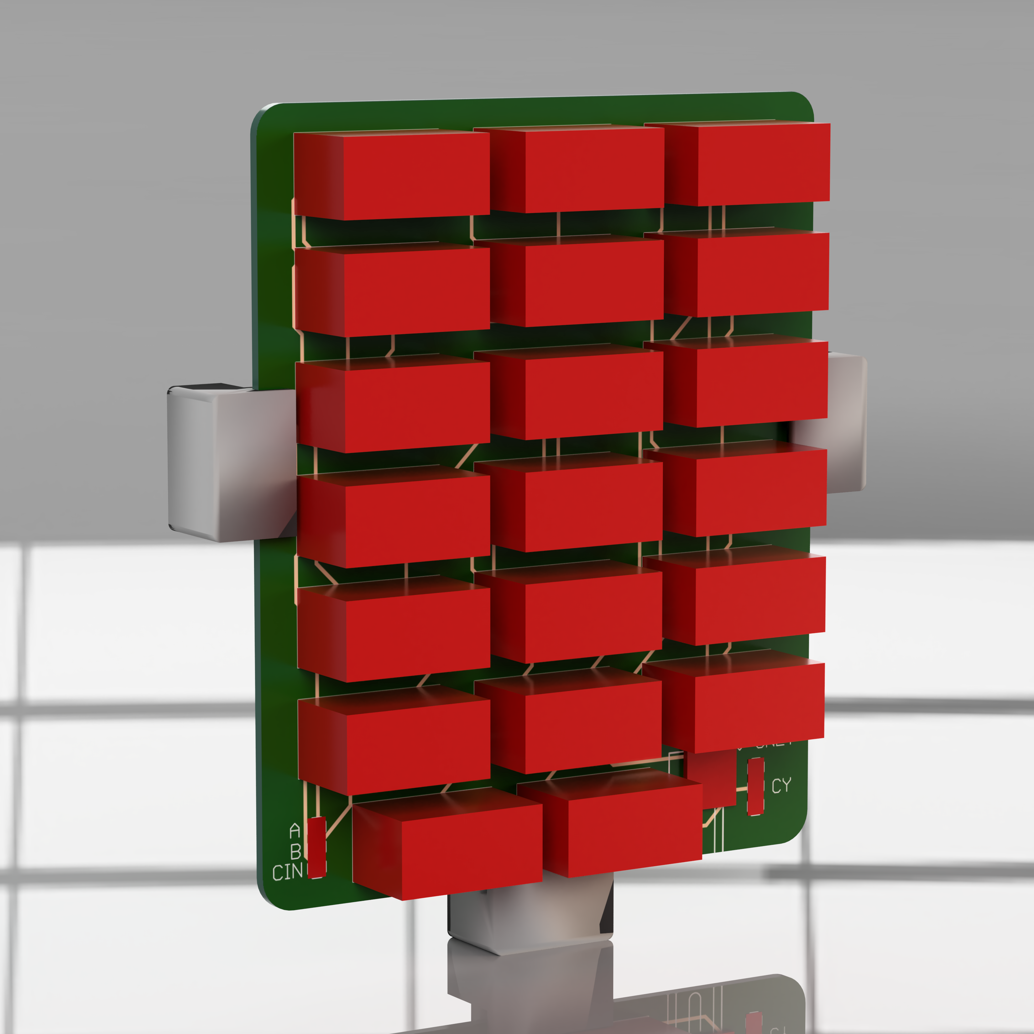
The design and fabrication of a custom PCB followed the creation of a full adder circuit diagram in EAGLE (PCB shown right, link to schematic image: https://goo.gl/cXBRqa). The next step, after the arrival of the PCBs, was soldering the components to the board and testing operation. This includes soldering yellow relays in such a way that the four boards together spell out the word "ACES".
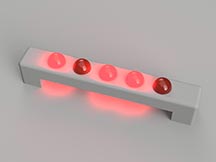 The next step was designing the LED holder (present below at right) and the clips used to mount the PCBs. Using Fusion 360 for design and the Ultimaker 3 for fabrication made this easy and efficient. This step included multiple iterations of the PCB clip design. The final product has an aesthetically pleasing symmetry, is easy to use and is strong.
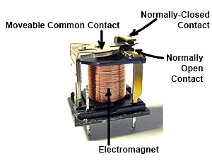 The next step is attaching the parts to the plywood board with the intention of making the final project both visually appealing and easy to use. This step consists of gluing the PCBs down using the custom designed clips and drilling holes through to the other side of the board to hide wires. It also includes soldering switches to power rails, chaining the CARRY OUT and CARRY IN pins of consecutive boards together, connecting the LEDs to the outputs of the full adder PCBs and labeling specific components for ease of use. The final step is connecting the full adder PCBs to the respective switch inputs. The project is now complete.
Media
 | 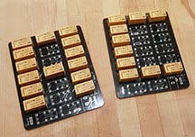 |
| Circuit board render with clips | Yellow relays soldered on boards A & C |
|---|---|
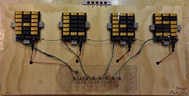 | 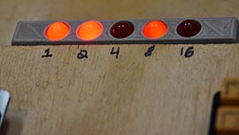 |
| Final Product | Output showing value of "11" |
| Link to YouTube Video: https://youtu.be/XpCeyXjMD98 | |
Conclusion
In conclusion, I am happy with the result of this project. I enjoyed working with relays, despite them not being my initial choice in the Yankee Swap. This project had the unique benefit of being a mini history lesson too. I learned, through research online, how relays used to be found in nearly all electronics prior to the widespread use of vacuum tubes and transistors. Through this project I also learned why relays are never used in logic applications anymore: they use a lot of power, are very expensive and are at risk of mechanical failure. I am also happy with the appearance of my final project and am happy that it is going to be displayed in the lab for potential and younger students to get excited about electronics. While there are many skills that this project did not require (coding being the most significant), I still believe that this project was a resounding success.
Reference
Lekule, Sostenes. "A Full-Adder." LEKULE BLOG, 21 Apr. 2015, http://sosteneslekule.blogspot.ca/2015/04/a-full-adder.html.
"Relay Logic Gates." Electro-Tech-Online.com, http://www.electro-tech-online.com/attachments/upload_2015-6-18_21-28-8-png.92993/.