NAND Gate Oscillator
Purpose
The purpose of this project is to create a square voltage wave using analog and digital logic. The square is to turn on and off an LED at varying rates and a set duration. The rates must vary based on the configuration of resistor-capacitor circuits in the NAND Gate Oscillator (NGO).
| Parts List | |
|---|---|
| 9V Battery or Power Supply | 4.7MΩ Resistor |
| DC Breakout Board | 10MΩ Resistor |
| Pushbutton Switch | 0.01µF Capacitor |
| Zener Diode | 0.1 µF Capacitor |
| 470Ω Resistor | 10µF Capacitor |
| 10KΩ Resistor | 4011 Quad 2-Input NAND Gate |
| 1MΩ Resistor | Blue 5mm LED |
| 2.2MΩ Resistor |
Procedure
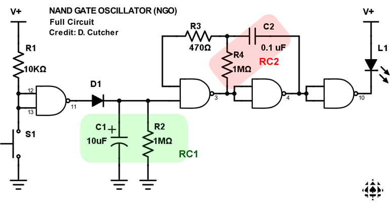
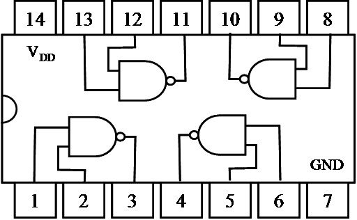
The project began with an overview of how a 4011 Quad input NAND Gate works. A 4011 Integrated Circuit (IC), like nearly all ICs requires a power source and a ground. The 4011 contains 4 separate NAND gates. The first NAND gate, as seen in fig. 1, receives input on pins 1 and 2. Pin 3 then outputs high or low based on the inputs. Inputs must be conditioned with distinct high and lows. The NGO uses a pushbutton switch and a pull up resistor to ensure conditioned inputs. The 4011 IC requires positive current on pin 14 and a ground connection on pin seven to work reliably. NAND gates face each other on both the top and bottom of the IC as seen in fig. 1. Pin numbering starts at the left below the notch and moves anti-clockwise.

The input of the NGO is the momentary press of the pushbutton switch. At rest, the first NAND gate receives two high signals and outputs a low signal. The positive current on pin 11 can sink itself into the IC. Pressing of the button delivers low signals on the input pins and the gate outputs a high signal. The positive current sitting on pin 11 flow. When the button is not pressed, an LED placed on pin 11 will illuminate.
The first resistor-capacitor (RC) circuit of the NGO determines how long the square wave in the final circuit will oscillate for. When pressing the button, the high signal from the first NAND gate grounds into the capacitor until the resistance of the capacitor is too great. The high current then moves into the second NAND gate and triggers a low signal output. This means that an LED placed on pin three of the IC will ground itself and illuminate. When the button is no longer pressed, the capacitor drains into the 1MΩ resistor and the NAND gate. A zener diode prevents back flow. When the charge provided by the capacitor is no longer half of the original input signal, the NAND gate registers two low inputs. The NAND gate now outputs a high signal and stops positive current from sinking into ground through the IC. When the button is pressed, an LED on pin three will illuminate and then stay lit when the button is no longer pressed and the capacitor supplies more than half the input voltage.
Test 1 | Test 2 | Test 3 | Average | |
|---|---|---|---|---|
2.2MΩ + 0.1 µF | 28 | 28 | 28 | 28.0 |
2.2MΩ + 0.01µF | 310 | 311 | 310 | 310.3 |
4.7MΩ + 0.1 µF | 13 | 13 | 13 | 13.0 |
4.7MΩ + 0.01µF | 150 | 150 | 150 | 150.0 |
10MΩ + 0.1 µF | 6 | 6 | 6 | 6.0 |
10MΩ + 0.01µF | 66 | 66 | 66 | 66.0 |
Note: All values are in flashes per 10 seconds unless otherwise stated | ||||
The final RC circuit of the NGO determines how fast the square wave oscillates. A high signal on the second NAND gate travels through R4 and fills up C2 until the resistance is more than 470Ω. The signal then feeds back on itself along with the duration circuit into the second NAND gate. If C1 is not drained, the second NAND gate receives two high signals and outputs low. C2 can now drain into NAND gate four and NAND gate 3 will output a high signal. This causes NAND gate four to output a low signal. When the capacitor no longer provides half the input voltage, one of the inputs to the second NAND registers a low signal and it outputs high again. The cycle repeats until the duration circuit provides less than half the input voltage and NAND gate two can no longer receive two high signals. Adjusting the capacitance of C2 and resistance of R4 will change the frequency of which an LED placed on pin 10 of the IC blinks. See the chart right for tests with different resistance and capacitance.
Media
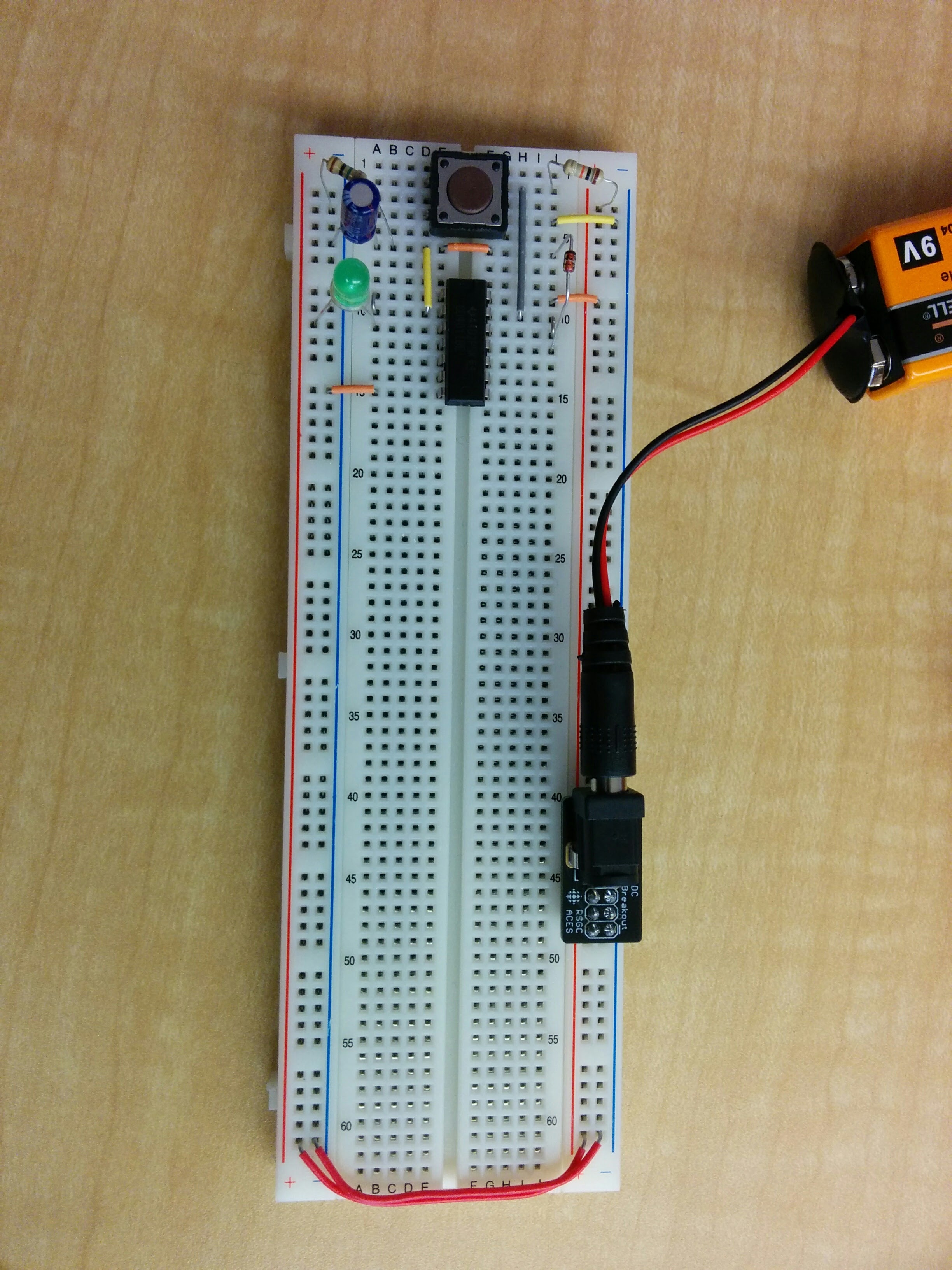
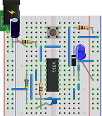 | 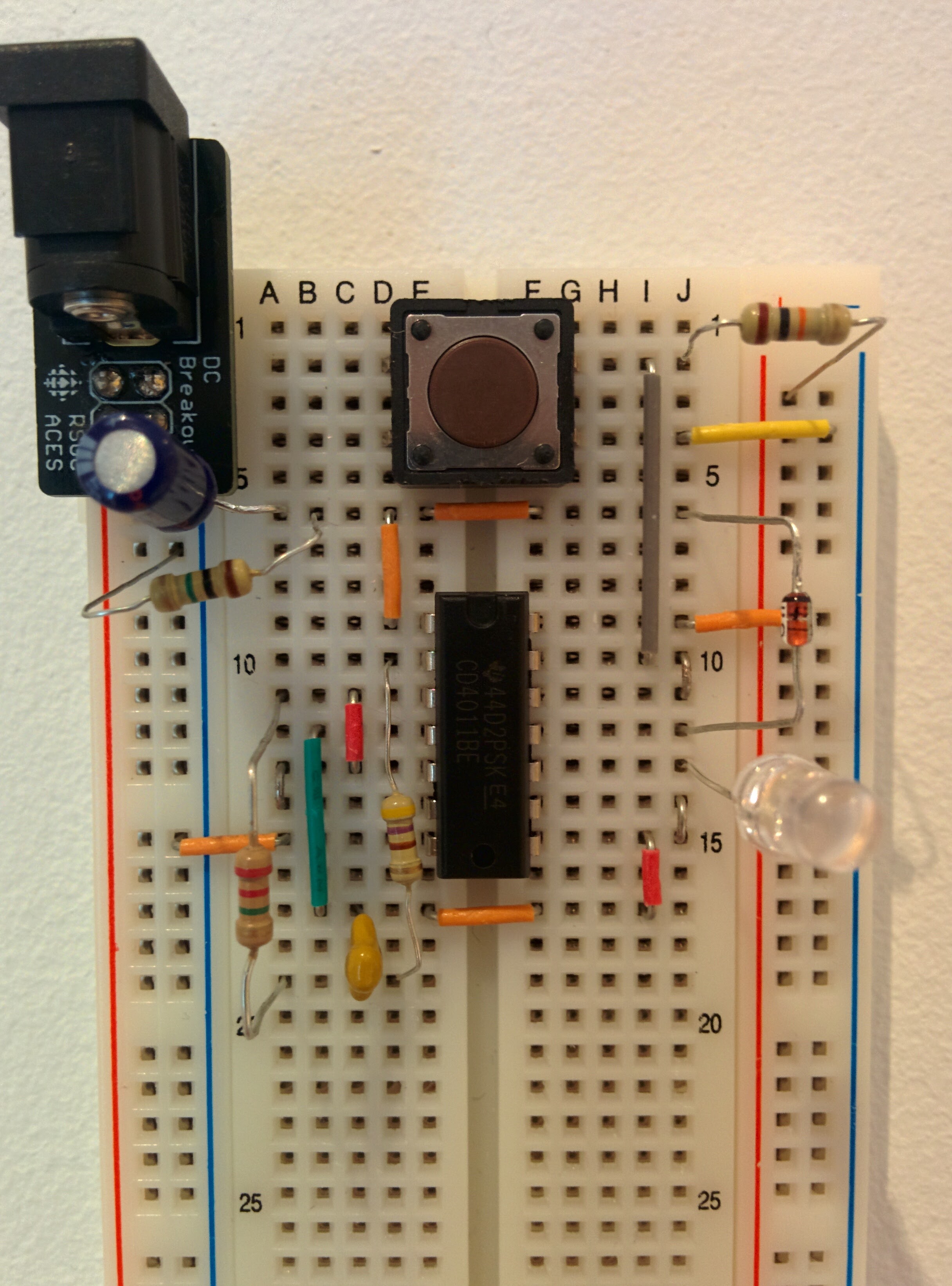 |
| Fritzing Diagram | Final circuit on breadboard |
|---|---|
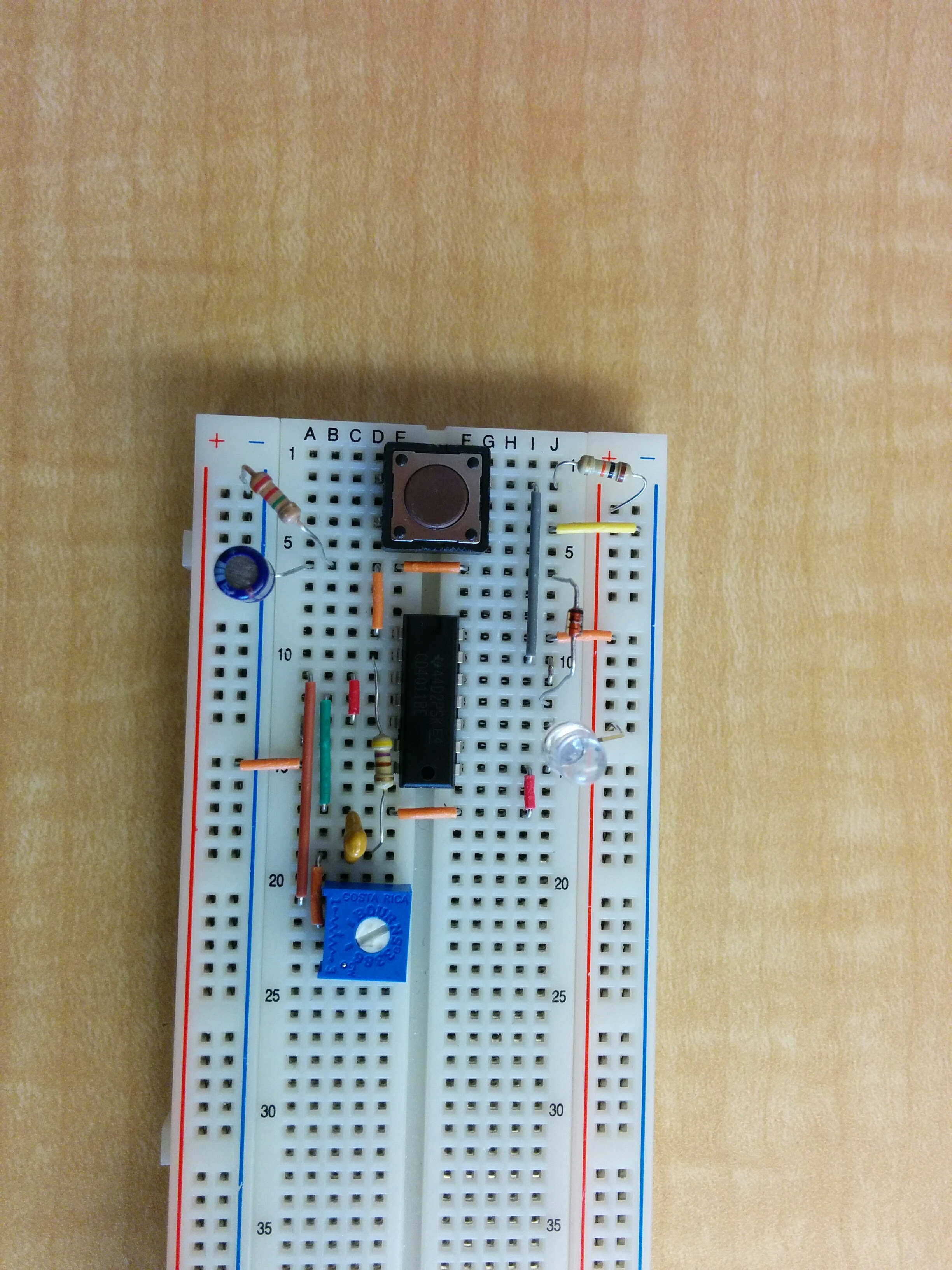 |  |
| Using a potentiometer in place of R4 | Duration circuit |
| Link to YouTube Video: https://www.youtube.com/watch?v=sy4HRHxsPOQ | |
Conclusion
In conclusion, this circuit taught me a lot about how digital logic works. I learned how integrated circuit boards work and how to properly use them. The project fulfils its purpose without fail. From this project, I learned that digital logic still relies heavily on smaller analog circuits. I enjoyed learning how to use tools like an oscilloscope and a high speed camera to see the square wave output of my NGO. It was quite satisfying to learn about possible usages for a square wave clock signal; the counting 7-segment display was especially fun to build. Overall, I believe that the amount of time I spent on this project was whole-heartedly worth it and is the main reason I was able to achieve the desired outcome.
Reference
Cutcher, D. NGOInput770W. Digital image. RSGC ACES. N.p., n.d. Web. 14 May 2016. http://darcy.rsgc.on.ca/ACES/TEL3M/images/NGOInput770W.png.
D'Arcy, Chris. "TEL3M Activities." RSGC ACES. N.p., n.d. Web. 14 May 2016. http://darcy.rsgc.on.ca/ACES/TEL3M/1516/TasksSpring.html#NGO.
Loomis, John. Digital image. Johnloomis.org. N.p., n.d. Web. 14 May 2016. http://www.johnloomis.org/ece201L/lab10/4011.jpg.
Kelley, Nicole. "Sentence Structure of Technical Writing." RSGC ACES. N.p., Fall 2006. Web. 14 May 2016. http://darcy.rsgc.on.ca/ACES/technical-writing.pdf.